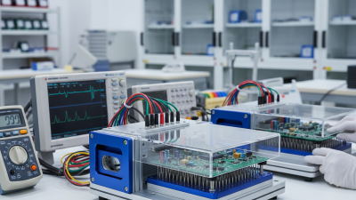
What is a PCB Test Jig and How Does It Work?
In the realm of electronics manufacturing, the significance of a "pcb test jig" cannot be overstated. Experts like Dr. Emily Chen, a renowned engineer in the PCB testing industry, emphasize its importance: “A well-designed PCB test jig is crucial for ensuring product reliability.” A PCB test jig serves as a specialized fixture that holds printed circuit boards during testing. It allows for accurate electrical measurements, ensuring that each component operates as intended.
The effectiveness of a PCB test jig lies in its design and setup. Each jig must cater to specific board layouts and testing requirements. This customization enhances the precision of the tests performed. Yet, there are challenges; if the jig is poorly designed, it can lead to inaccurate readings. Therefore, attention to detail is key.
As technology advances, the role of PCB test jigs evolves too. New testing methodologies require upgrades and refinements in jig design. There is always room for improvement. Industry professionals must continually assess current jigs to keep pace with innovation. The demand for reliability in electronic devices makes this ongoing evaluation essential.
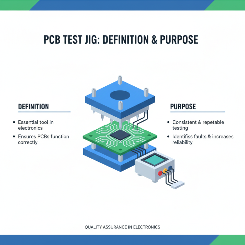
Definition and Purpose of a PCB Test Jig
A PCB test jig is an essential tool used in the electronics industry. It is designed to ensure that printed circuit boards (PCBs) function correctly before they are integrated into larger systems. The main purpose of a test jig is to provide a consistent and repeatable testing environment. This helps identify any faults in the PCB, increasing reliability in the final product.
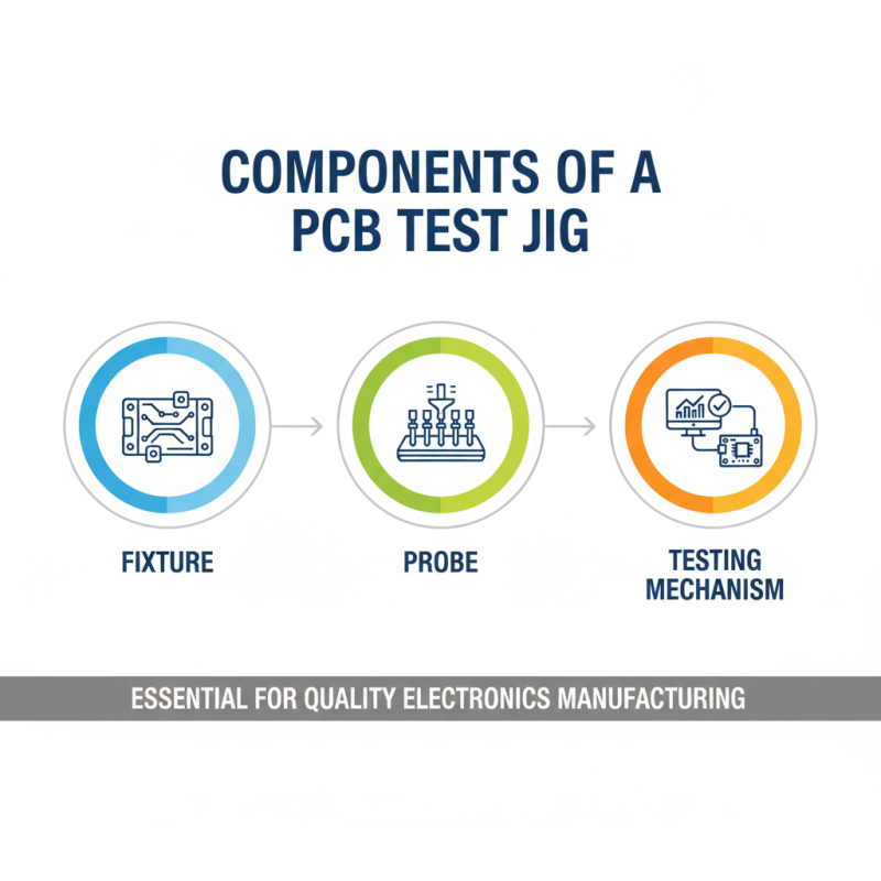
The design of a test jig typically involves a fixture that holds the PCB in place while it undergoes various tests. These tests can check electrical functionality, signal integrity, and even mechanical durability. A well-made jig accommodates multiple PCB designs, but there can be limitations. Some jigs may not test every possible condition or interaction. For complex circuits, this can lead to oversights.
Professionals in the field must continually evaluate the effectiveness of their test jigs. They need to ask whether the testing procedures capture all potential faults. Frequent reflections on testing results can lead to better design and testing methods. A rigorous approach to using and improving test jigs ultimately enhances the quality of PCBs produced.
Working Principle of a PCB Test Jig
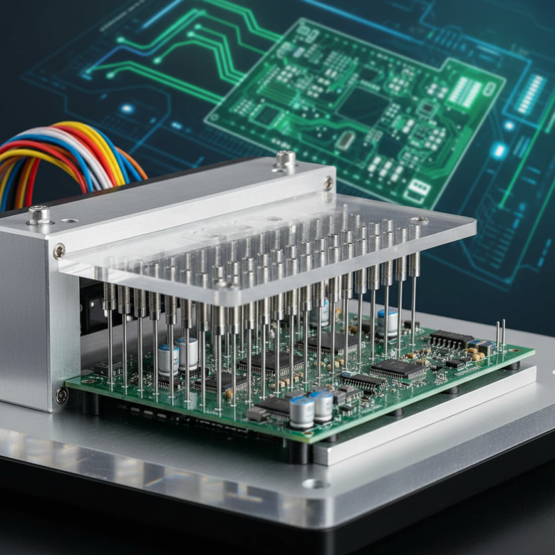
A PCB test jig plays a crucial role in the quality assurance of electronic devices. Its primary purpose is to facilitate the testing of printed circuit boards (PCBs) for functionality and performance. Typically, these jigs are designed to hold the PCB in place while interfacing with testing equipment. This setup enables precise measurement of electrical signals, identifying faults before products hit the market.
The working principle of a PCB test jig revolves around the concept of connectivity and signal integrity. Test probes are strategically placed to connect with various points on the board. According to a report from IPC, approximately 80% of defects occur during manufacturing. A well-designed jig can help to uncover these issues early. The test jig can simulate real-world operating conditions, creating scenarios for thorough validation.
Moreover, employing a test jig can lead to efficiency gains. A study by the IEEE indicates that automated testing can reduce test time by up to 50%. This improvement allows for quicker turnarounds in production. However, challenges remain. Designing a jig that accommodates multiple board layouts can introduce complexity. Achieving a balance between robustness and adaptability is an ongoing concern in the industry. Testing methodologies continue evolving, emphasizing the need for continual improvement in jig design.
PCB Test Jig Specifications
| Parameter |
Value |
Description |
| Test Jig Type |
Manual |
Jig operated by user intervention |
| Pin Count |
50 |
Number of test pins available |
| Test Voltage |
5V |
Voltage applied during testing |
| Temperature Range |
-10°C to 60°C |
Operating temperature for testing |
| Test Duration |
5 minutes |
Time taken to complete a test cycle |
| Data Output |
CSV Format |
Format for exporting test results |
Types of PCB Test Jigs and Their Applications
PCB test jigs come in various types, each tailored to specific testing needs. One common type is the functional test jig. This jig checks if the printed circuit board (PCB) operates as intended. It connects to the PCB's components and simulates real-world functioning conditions. Users must ensure the jig interfaces properly to gather accurate results. If any mismatch occurs, it can lead to misleading data.
In-circuit test jigs focus on testing the individual components on the PCB. This type can identify faulty components quickly. Each connection must align precisely to facilitate accurate measurements. Designers face challenges in creating jigs that are both efficient and adaptable. Oftentimes, they must redesign jigs for new PCB layouts. This can lead to increased costs and time delays in the manufacturing process.
Automated test jigs are becoming popular in larger production runs. These jigs can significantly reduce human error, but they also require complex software and calibration. Security and reliability of the automated process can introduce concerns. Engineers must continuously refine their setups for efficiency. Each type of PCB test jig presents its own set of advantages and challenges. Understanding these nuances can enhance performance in testing environments.
Benefits of Using a PCB Test Jig in Electronics Testing
A PCB test jig is an essential tool in electronics testing. It standardizes the process of verifying the functionality and quality of printed circuit boards. Using a test jig can significantly streamline the testing procedure. It ensures that each board is subjected to the same tests, which helps maintain consistency in results.
One major benefit of using a PCB test jig is its capability to detect defects early. This early detection can save time and resources. Issues can be identified before they escalate into larger problems. A well-designed jig can target specific areas of a PCB, ensuring precise testing and reliable outcomes. However, not all test jigs are created equal. Some may not adequately cover all functionalities, leading to possible oversights.
Moreover, a test jig can improve testing efficiency. It reduces the time taken for manual inspection. Technicians can focus on interpreting the results rather than conducting repetitive tasks. Yet, it is crucial to continuously assess the jig's design and functionality. Regular updates and improvements may be required to keep pace with evolving technology. This reflection can optimize the testing process, ensuring that electronic devices meet quality standards.