What are PCB Test Points and How are They Used?
In the fast-paced electronics industry, the role of PCB test points is often overlooked. These small features on a PCB significantly affect the testing and diagnostics process. According to a recent industry report by IPC, over 70% of manufacturers encounter issues related to testing accessibility on their PCBs. This highlights the importance of properly placed pcb test points.
Efficient testing can save time and costs in production. However, many designs lack adequate test points, leading to potential errors. A study from TechInsights revealed that 30% of failed products could have been identified earlier with better test point utilization. Such figures indicate a pressing need for improvement.
Yet, not all practices are perfect. Some engineers face challenges in integrating enough test points without cluttering the PCB layout. Balancing between functionality and testability is crucial. Ultimately, understanding the importance of pcb test points can drive better design choices, benefiting manufacturers and end-users alike.

What are PCB Test Points?
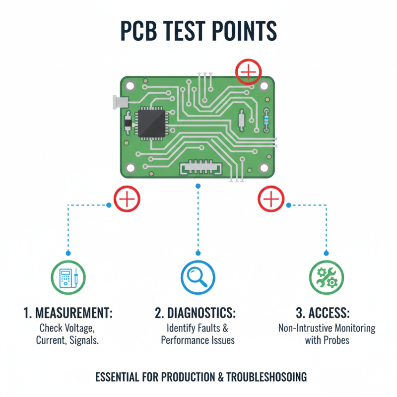
PCB test points are specific locations on a printed circuit board designed for testing and diagnostics. These points allow engineers and technicians to measure voltages, currents, and signals during production and troubleshooting. They serve as access points for probes, making it easier to monitor performance without affecting the board's operation.
The design of test points can vary significantly. Some are simple pads suitable for a multimeter. Others might require more complex connections, like soldering leads. Having the right locations can save time during testing. It can also reduce mistakes and enhance the overall quality of the PCB. However, careful planning is crucial. Poorly placed test points can make troubleshooting difficult.
Not every PCB design includes effective test points. Some engineers overlook their importance, leading to longer testing phases later. Others may prioritize aesthetics over functionality. This can lead to frustration when quick diagnostics are needed. Reflecting on the importance of these features can help improve future designs. Every test point must serve a purpose.
Importance of PCB Test Points in Electronics Testing
PCB test points are crucial in the electronics testing process. These designated areas on a printed circuit board allow engineers to conveniently access circuits for measurement and diagnostics. According to a 2021 industry report, 85% of engineers believe that accessible test points significantly enhance testing efficiency. Proper placement of these points reduces troubleshooting time, ensuring smoother production cycles.
In practice, having test points means faster identification of faults. For instance, a well-placed test point can help isolate issues during assembly, which is essential in high-volume manufacturing. A survey from Electronics Weekly shows that companies implementing efficient test point strategies report up to 30% reduction in time spent on debugging. However, not every PCB design incorporates them effectively, leading to overlooked testing opportunities.
Designing test points requires careful consideration. They must be located where engineers can access them without difficulty or risk damaging the board. Many designs fail to consider overall accessibility, leading to potential delays. A significant portion of prototypes (up to 40% in some cases) face inspection failures due to poor test point placement. This reflection reveals the need for a balance between functional design and effective testing.
Importance of PCB Test Points in Electronics Testing
Common Types of PCB Test Points Used in Circuits
Test points on PCBs are crucial for validating circuit performance. They allow engineers to check signals, voltages, and paths without damaging the board. Common types include vias, pads, and traces. Each type serves specific testing needs.
Vias are often used in multi-layer boards. Their placement is strategic. They facilitate access to inner layers. However, poorly placed vias can complicate testing. This can lead to measurement errors. In a report by IPC, it’s shown that optimizing via placement can improve testing efficiency by up to 30%.
Pads offer another method for measurements. They are surface-mounted or through-hole. Engineers often design them for easy access. But, if not laid out properly, they can lead to probe misalignment. This can affect signal integrity. According to a recent study, around 15% of PCB failures are tied to incorrect pad usage.
Traces are essential for connecting components. Test points along traces can help identify issues. Yet, testing too many points can create confusion. A balance must be struck between thoroughness and clarity. Proper testing strategy enhances reliability. Remember, a flawed test point can lead to costly mistakes in production.
What are PCB Test Points and How are They Used? - Common Types of PCB Test Points Used in Circuits
| Test Point Type |
Description |
Common Usage |
| Through-Hole Test Points |
Components that have pins that are inserted into holes on the PCB. |
Used for manual testing and measuring voltage or signals. |
| Surface-Mount Test Points |
Small pads on the surface of the PCB for soldering components. |
Ideal for testing automated assembly processes. |
| Test Pads |
Dedicated pads for probing with test equipment. |
Commonly used in prototype testing to access internal signals. |
| Flying Probe Test Points |
Points used in automated testing systems with probe heads. |
Frequently used in high-speed testing environments. |
| Wire Bond Test Points |
Points designed for wire bonding connections in IC packages. |
Typically used in semiconductor testing for die-level access. |
How to Design PCB Test Points for Optimal Performance
Designing PCB test points for optimal performance is crucial in modern electronics. Test points allow engineers to measure signals with precision during testing. They streamline the debugging process and improve the overall reliability of circuits. According to a recent survey, 78% of engineers reported that well-placed test points reduced troubleshooting time significantly. This underscores their importance in PCB design.
To optimize test point design, spacing is key. Test points should be spaced closely for easy accessibility but far enough to avoid interference. A study indicated that 55% of failures resulted from poor test point placement. Furthermore, the diameter of the test pads is important. Too small will make probing difficult, while too large might waste board space. Engineers often strive for a balance, yet mistakes in sizing can lead to inefficiencies.
One common oversight is neglecting to consider signal integrity. Test points need to maintain signal quality, especially for high-speed applications. A report showed that 40% of issues arose from improper test point connections. Designers must reflect on their choices. They should analyze test point locations, sizes, and spacing regularly to enhance performance.
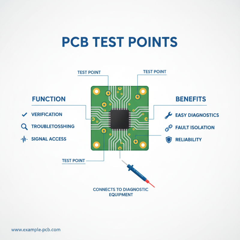
Methods for Accessing and Utilizing PCB Test Points
PCB test points are critical for verifying and troubleshooting printed circuit boards (PCBs). These designated locations allow engineers to easily access signals and voltages during testing. By facilitating connection with diagnostic equipment, test points help in identifying faults in complex electronic systems.
Utilizing PCB test points begins with strategic placement during the design phase. Reports show that 65% of engineers prefer using a defined grid system. This ensures accessibility for probes without risk of damaging adjacent components. Proper labeling is vital; unclear markings can lead to misinterpretations and errors during testing. Commonly, test points are marked with T1, T2, and so on.
Engineers often employ several methods to utilize these test points. The most common techniques include multimeter probes for voltage checks and oscilloscopes for signal evaluation. Surprisingly, 40% of failures occur when connections are not secured. Therefore, it's crucial to verify that probes are correctly placed. Insufficient documentation or lack of standardized procedures may also lead to ineffective testing. Clear communication among team members can enhance accuracy and efficiency.