In the ever-evolving electronics industry, the importance of a test PCB cannot be overstated. A test PCB, or printed circuit board, is essential for validating designs before mass production. Renowned expert Dr. Emily Carter from Circuit Innovations emphasizes, "Test PCBs are the backbone of reliable electronic devices." This highlights their critical role.
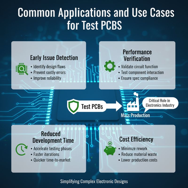
Test PCBs serve several purposes. They help engineers catch errors, reduce costs, and ensure functionality. Imagine a smartphone that can’t connect to the internet. Such issues can stem from overlooked flaws in the PCB design. Developing an effective test PCB involves careful planning. It needs to reflect the final product accurately. Any discrepancies can lead to major setbacks.
However, many professionals struggle to prioritize the design of test PCBs. This reflection is crucial. A lot of time can be wasted on prototypes that don't address underlying flaws. Each iteration should be a step closer to a reliable final product. Neglecting the test PCB phase can result in costly recalls and damaged reputations. A rigorous test PCB process is crucial for success in the electronics market.
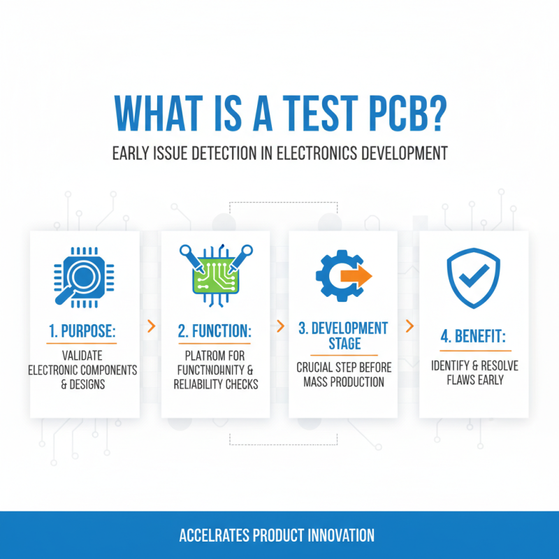
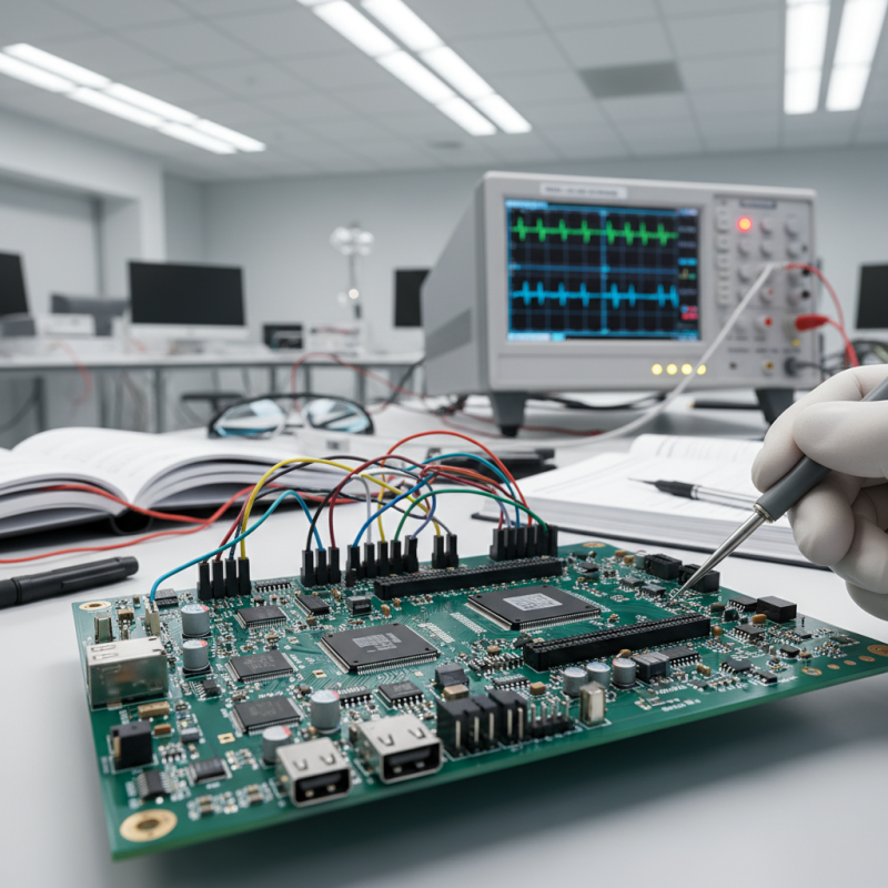
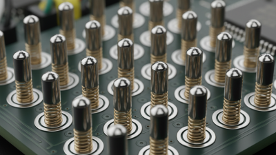
A Test PCB, or Printed Circuit Board, is designed specifically for testing electronic components. This type of PCB provides a platform for engineers to test the functionality and reliability of their designs. It serves as a crucial step in the development process. By using a Test PCB, teams can identify issues early on in production.
When it comes to a Test PCB, functionality is key. These boards are often simpler than final production PCBs. They are designed to facilitate easy access to critical points. This allows for quick measurements and alterations. Engineers can troubleshoot problems with precision. They can often modify circuits on the fly, which improves testing efficiency.
However, not all Test PCBs are perfect. Sometimes, designs may experience unexpected failures. This can lead to frustration and delays. Engineers should be prepared to adapt and rethink their strategies. The goal is to create a reliable product, which requires diligence and a willingness to learn from mistakes. Each iteration provides valuable insights that shape future designs.
A Test PCB plays a crucial role in electronic development. It serves as a platform for testing and debugging electronic circuits before moving to mass production. Typically, engineers use these boards to verify design functionality and identify any potential issues. This early-stage testing can save time and resources in later product phases.
During the testing phase, engineers can evaluate various components. They can monitor voltage levels and check signal integrity. However, not every test yields perfect results. Sometimes, unexpected issues arise, leading to further refinements. This process can be frustrating but ultimately leads to better designs. Engineers must remain patient and adaptable when changes are necessary.
The significance of Test PCBs cannot be overstated. These boards help shape reliable electronics in the long run. They allow for iterative learning, where engineers can reflect on failures and successes. Each iteration brings the design closer to the final product. However, it is essential to document each outcome, as this knowledge builds a stronger foundation for future projects.
A Test PCB, or printed circuit board, is crucial in the electronic design process. Its primary function is to evaluate prototypes before mass production. Test PCBs help identify design flaws early. This can save time and resources in product development.
Key features of a Test PCB include versatile routing and multiple test points. These facilitate easy access for measurement and troubleshooting. Test PCBs often have extra pads and vias for connection flexibility. This is key for adapting designs to various testing scenarios.
Another significant feature is their ability to accommodate different components. This includes both surface mount and through-hole parts. However, balancing spacing and layout can be challenging. Designers may struggle with component placement. Mistakes here can lead to testing errors. A good Test PCB should encourage iteration and improvement, making room for refinement.
The Test PCB plays a crucial role in ensuring product reliability and performance. This chart displays the importance levels of various key features of a Test PCB, such as Signal Integrity, Thermal Conductivity, Testing Flexibility, Cost-Effectiveness, and Time to Market, rated on a scale of 1 to 10.
Test PCBs play a crucial role in the prototyping phase of electronic device development. These specialized boards allow engineers to validate designs before mass production. According to industry reports, around 45% of development delays stem from design flaws. Using test PCBs significantly reduces this risk. They help identify errors in layout, component placement, and connectivity early in the process.
The benefits are clear. Test PCBs save time and money. They allow for rapid iterations, ensuring that mistakes are caught before they escalate. In one study, companies reported a 30% reduction in prototype costs when using test PCBs. This improvement is vital, especially in markets where speed to market is a competitive advantage. However, not all engineers fully utilize test PCBs. Anecdotal evidence suggests that many skip this step, believing it adds unnecessary time. This is a misconception that can lead to costly redesigns later.
Moreover, the flexibility of test PCBs allows for testing various configurations. Engineers can explore different designs without committing to a final version. This adaptability fosters creativity but can also lead to analysis paralysis. Some teams may become overwhelmed by options and forget the project’s core functions. It’s a balancing act between thoroughness and efficiency, yet the benefits often outweigh the potential pitfalls.
Test PCBs play a critical role in the electronics industry. They are designed to verify the performance of circuit boards before mass production. With complex electronic designs, test PCBs help identify potential issues early. This reduces costs and shortens development timelines.
Common applications for test PCBs include automotive, telecommunications, and consumer electronics. In the automotive sector, they ensure that critical systems function properly. Data from industry reports show that the test PCB market is expected to grow at a rate of 5.1% annually until 2027. This growth reflects increasing demands for reliability and performance across various sectors.
Tips: When designing a test PCB, consider the types of components you will use. Keep your layout simple to avoid confusion. Avoid overcrowding traces, as this can lead to errors during testing. Remember, the goal is clarity and functionality. Regularly review designs to catch mistakes early. It’s better to learn from small errors than to face larger issues later.