
Top PCB Testing Methods for Global Buyers
Global electronics production is becoming more complex, faster, and less forgiving. The World Semiconductor Trade Statistics (WSTS) forecast global semiconductor sales at approximately US$611 billion in 2024, with further growth expected in 2025. More devices mean denser boards, tighter tolerances, and greater pressure on supplier quality. For international buyers, selecting suitable pcb testing methods is not a minor purchasing detail. It directly affects field reliability, warranty exposure, and delivery confidence.
IPC standards provide a practical foundation for evaluation. IPC-A-600 defines printed board acceptance criteria, while IPC-A-610 supports electronic assembly workmanship assessment. IPC-9252 also addresses electrical test requirements for printed boards. Common approaches include automated optical inspection, in-circuit testing, flying-probe testing, functional testing, and X-ray inspection. Each method reveals different defects. AOI can identify solder bridges and component misalignment. X-ray inspection can expose hidden voids beneath BGA packages. Flying probes offer flexibility when production volumes change.
There is no universal winner.
IPC industry surveys continue to show that manufacturers face cost, labor, supply-chain, and capacity pressures. These conditions can influence test depth and sampling decisions. Buyers should therefore request measurable evidence, including defect coverage, test-point access, false-call rates, calibration records, and corrective-action history. A capable supplier should explain both detection limits and inspection results. That honesty matters. A test strategy can still miss intermittent faults, especially when fixtures, software, or operator judgment are weak. Global buyers should compare methods against product risk, volume, technology, and destination-market requirements, rather than choosing the lowest quoted inspection cost.
Why PCB Testing Matters for Global Buyers
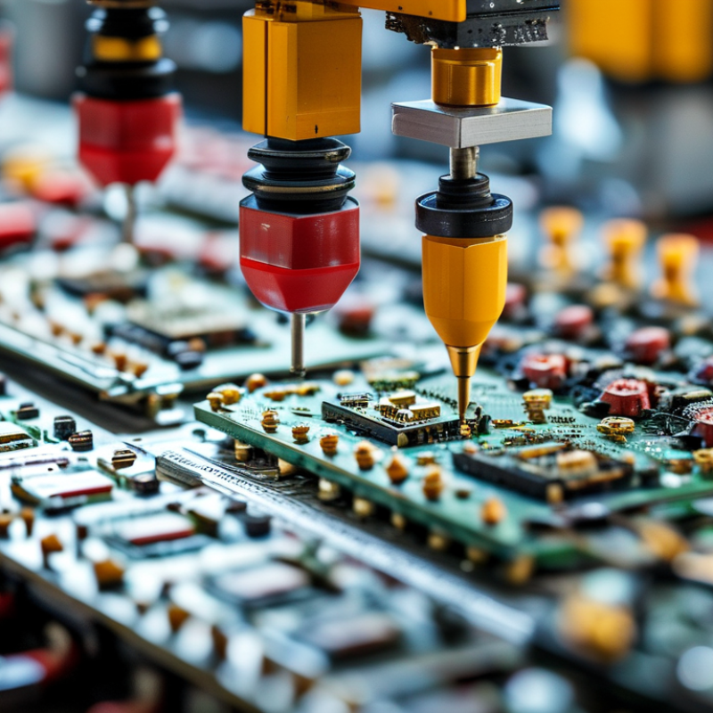
For global PCB buyers, testing is not a paperwork exercise. It protects product performance across factories, climates, and shipping routes. A board may pass visual inspection yet fail when a tiny solder void heats under load. Testing exposes hidden defects before they become field returns, production delays, or safety concerns. It also gives purchasing teams objective evidence, not optimistic claims.
A practical program can combine automated optical inspection, flying-probe checks, in-circuit testing, and functional testing. X-ray inspection helps examine concealed joints, while impedance testing confirms high-speed signal paths. Thermal cycling can reveal weak vias after repeated expansion and contraction. Reliable suppliers should provide test records, lot identification, equipment calibration dates, and clear acceptance limits. Requirements should match the final application and relevant regulations. One generic test plan is rarely enough.
Tips: Ask for a sample inspection report before placing a large order. Confirm whether testing covers bare boards, assembled boards, or both. Define retest rules and nonconformance handling in writing. Keep approved samples for comparison. Do not treat a perfect first batch as permanent proof; processes drift, and even experienced teams can miss an unusual failure. That uncertainty deserves attention.
Top PCB Testing Methods for Global Buyers - Why PCB Testing Matters for Global Buyers
A practical comparison of common PCB testing methods used to verify quality, reliability, compliance, and production consistency across international supply chains.
| Testing Method | Main Purpose | Typical Defects Detected | Best Production Stage | Typical Coverage | Value for Global Buyers | Key Limitation |
|---|---|---|---|---|---|---|
| Automated Optical Inspection (AOI) | Visual verification of solder joints, component placement, and PCB assembly features. | Missing or misplaced components, solder bridges, insufficient solder, polarity errors, and visible trace defects. | After solder paste printing, component placement, and reflow soldering. | High-speed inspection of nearly 100% of accessible assembly areas. | Creates digital inspection records and helps identify process variation before shipment. | Cannot reliably inspect hidden solder joints beneath most area-array packages. |
| X-Ray Inspection | Non-destructive inspection of internal structures and concealed solder connections. | Voids, head-in-pillow defects, insufficient solder, solder bridges, detached connections, and hidden vias. | After assembly, especially for complex or high-density boards. | Sample-based or full inspection, depending on product risk and equipment capacity. | Reduces the risk of shipping assemblies with hidden failures that visual inspection cannot detect. | Higher equipment and operating costs; image interpretation requires trained personnel. |
| In-Circuit Test (ICT) | Electrical verification of individual components and circuit connections using test probes. | Open circuits, short circuits, wrong component values, missing components, and certain power faults. | After assembly and soldering. | Broad component-level coverage when suitable test access is available. | Provides objective electrical data and supports consistent acceptance decisions across suppliers. | Requires a dedicated fixture, which can increase initial cost and setup time. |
| Flying Probe Test | Probe-based electrical testing without a fixed production fixture. | Continuity failures, shorts, incorrect resistance or capacitance, and many assembly connection errors. | Prototype, engineering validation, and low-to-medium-volume production. | Good test access for exposed test points and conductive nodes. | Avoids fixture investment and is useful when designs or suppliers change frequently. | Generally slower per board than fixture-based ICT for high-volume production. |
| Functional Test | Confirms that the completed PCB performs its intended electrical and operational functions. | Firmware loading errors, interface failures, incorrect outputs, communication faults, and system-level malfunctions. | Final assembly inspection and end-of-line production testing. | Application-dependent; covers complete operating behavior rather than every individual component. | Shows whether the product works as expected under defined operating conditions before international shipment. | May not identify the exact component or connection causing a failure. |
| Continuity and Isolation Test | Verifies that intended conductive paths are complete and unintended connections are absent. | Open traces, short circuits, incorrect net connections, and insulation breakdown between conductors. | Bare-board inspection before component assembly, and as part of assembly testing. | Can test essentially all defined nets when suitable access points are designed in. | Prevents defective bare boards from entering assembly and reduces avoidable rework costs. | Does not confirm component value, solder quality, or complete product functionality. |
| Burn-In and Environmental Stress Testing | Evaluates reliability under extended operation, temperature, humidity, vibration, or thermal cycling. | Early-life failures, thermal weaknesses, intermittent connections, material problems, and moisture-related issues. | Qualification, reliability validation, and controlled production sampling. | Sample-based testing is common; test duration varies according to product and risk level. | Supports risk control when products must operate reliably across different climates and transport conditions. | Adds time and cost and may require specialized chambers or fixtures. |
| Microsection Analysis | Destructive examination of a cross-section to verify internal construction and workmanship. | Plating voids, inadequate copper thickness, delamination, barrel cracks, poor solder fillets, and layer-registration problems. | Supplier qualification, process audits, failure analysis, and periodic quality verification. | Sample-based because the inspected board is normally destroyed. | Provides physical evidence for resolving disputes and verifying construction against drawings and specifications. | Destructive, time-consuming, and unsuitable for checking every shipped board. |
Related Posts
-

5 Innovative PCB Test Fixture Solutions for Efficient Circuit Board Testing
-

Top 10 PCB Testing Software for Quality Assurance in Electronics?
-
What is a PCB Test Jig and How Does It Work?
-
Top 10 PCB Test Jigs You Need for Perfect Testing?
-
10 Essential Tips for Designing an Effective PCB Test Jig
-

Ultimate Guide to PCB Test Jig for Efficient Circuit Testing in 2025