Understanding Wafer Probing Techniques for Enhanced Semiconductor Performance
In the rapidly evolving landscape of semiconductor manufacturing, wafer probing has emerged as a crucial technique for ensuring the performance and reliability of integrated circuits. This process involves the electrical testing of semiconductor wafers before they are diced into individual chips, allowing engineers to identify defects and optimize yield rates. As the industry pushes toward miniaturization and increased functionality, understanding the nuances of wafer probing techniques becomes paramount.
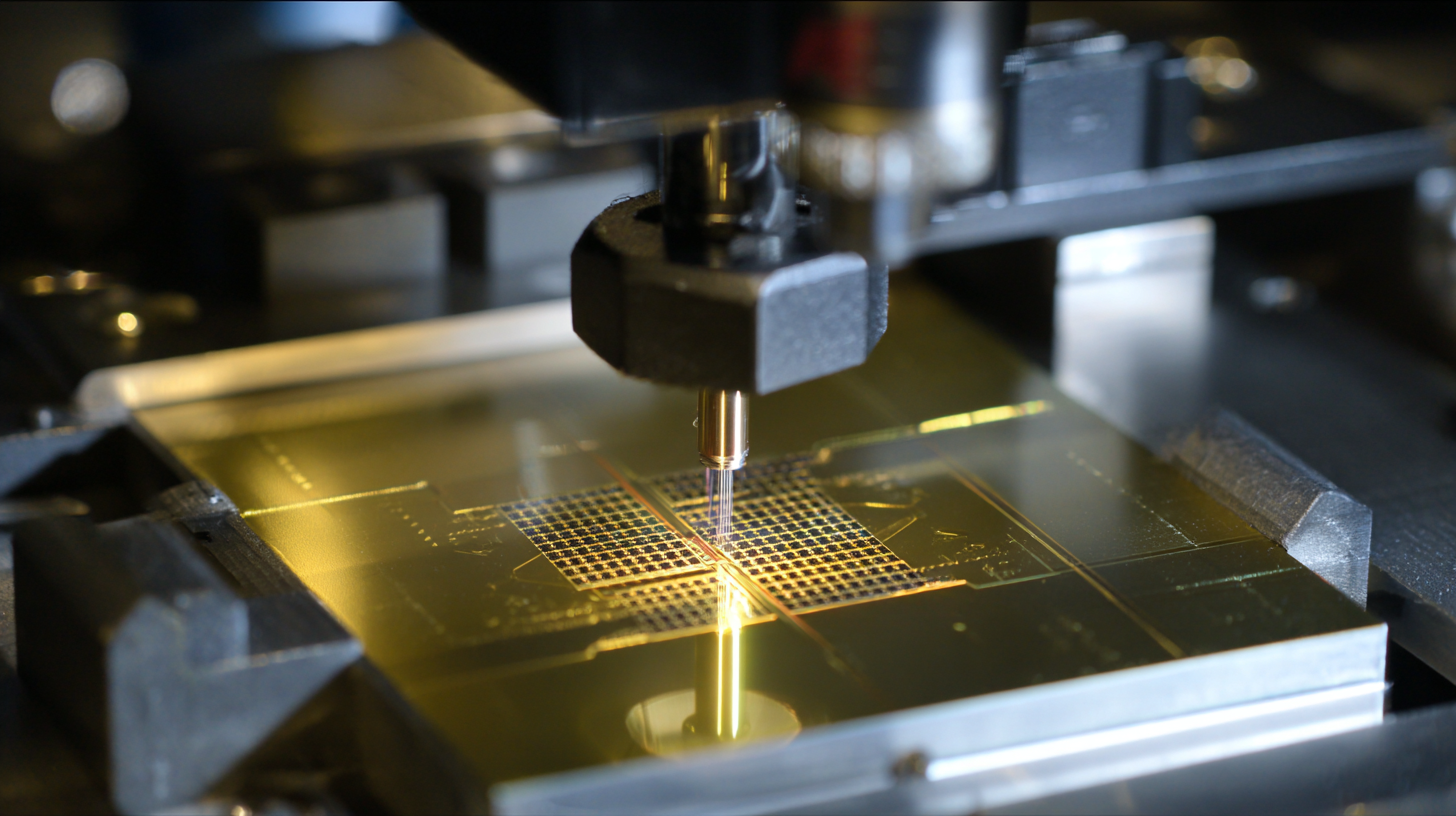
This introduction provides insights into the various methodologies employed in wafer probing, the technological advancements driving these practices, and their implications for enhanced semiconductor performance. By exploring the diverse types of wafer probing, from conventional mechanical methods to innovative contactless approaches, we aim to highlight how these techniques contribute to the overall efficiency and effectiveness of the semiconductor manufacturing process.
Recent Advances in Wafer Probing Techniques and Their Impact on Semiconductor Yield
Recent advancements in wafer probing techniques have significantly enhanced semiconductor yield, a critical factor in the ever-evolving electronics industry. According to a report by Yole Développement, the global semiconductor market is projected to reach $1 trillion by 2030, underscoring the dire need for efficient testing methodologies to improve production efficiency and reduce costs. Enhanced wafer probing not only accelerates the testing process but also increases the accuracy of detecting defects before the chips reach the packaging stage, thereby optimizing output.
Moreover, innovations such as micro-probing and advanced automated test equipment (ATE) have been pivotal. A study by SEMI indicated that automated wafer testing can reduce overall production costs by up to 25% while increasing throughput. The implementation of these advanced probing technologies enables more precise measurement of electrical characteristics at the wafer level, which contributes to improved yield rates. As semiconductor devices shrink and complexity rises, refining these probing techniques is essential to maintaining high-quality standards and ensuring competitive performance in the market.
Key Parameters Influencing Wafer Probing Performance in High-Volume Production
Wafer probing is a critical step in the semiconductor manufacturing process, especially in high-volume production environments. Several key parameters significantly influence wafer probing performance, leading to enhanced overall yields and device reliability. Firstly, the choice of probe card is paramount. A well-designed probe card ensures accurate electrical contact with the die, minimizing signal integrity issues. Factors such as probe needle material, tip geometry, and spacing must be carefully optimized to reduce contact resistance and prevent mechanical damage to delicate semiconductor structures.
In addition to the probe card design, the environment in which probing occurs plays a crucial role. Temperature control is essential; variations can impact both the physical characteristics of the wafer and the electrical properties being measured. Furthermore, the alignment accuracy between the probe and the wafer is vital. Any misalignment can lead to inconsistent results and increased scrap rates.
As manufacturers continue to push for higher throughput and improved performance of semiconductor devices, understanding and optimizing these parameters will be essential in mastering wafer probing techniques.
Comparative Analysis of Contact and Non-Contact Probing Methods for Chip Testing
In the realm of semiconductor testing, the choice between contact and non-contact probing methods can significantly impact the overall performance and reliability of chips. Contact probing, which involves direct physical contact with the chip surface, offers benefits such as lower resistance and better signal integrity. According to a recent report by Gartner, contact probing methods can achieve a contact resistance as low as 10 milliohms, which is crucial for high-frequency applications. However, the downside includes potential damage to delicate chip surfaces and increased wear over time, making it less ideal for advanced packaging technologies.
On the other hand, non-contact probing continues to rise in popularity due to its ability to test without physical interference. Utilizing optical or electromagnetic techniques, non-contact methods can minimize the risk of chip damage while facilitating faster testing speeds. A study published in the IEEE Transactions on Semiconductor Manufacturing indicated that non-contact probing can increase throughput by up to 40%, making it an attractive option for mass production environments. As semiconductor technology progresses further into smaller nodes, the consideration of probe methods will be pivotal in achieving optimal performance and reliability for next-generation devices.
Understanding Wafer Probing Techniques for Enhanced Semiconductor Performance
| Probing Method | Advantages | Disadvantages | Typical Applications | Cost Estimate |
|---|---|---|---|---|
| Contact Probing | Highly accurate measurements, Low contact resistance | Potential damage to delicate chips, Limited probe access | High-frequency testing, Small form factor chips | $10,000 - $50,000 |
| Non-Contact Probing | No risk of physical damage, Greater access to chip areas | Lower measurement accuracy, Higher complexity | Packaging tests, Advanced packaging technologies | $20,000 - $70,000 |
| Hybrid Probing | Combines benefits of both methods, Flexible usage | Increased system complexity, Higher costs | Mixed-signal testing, High-density chips | $30,000 - $80,000 |
Importance of Test Data Integrity in Wafer Probing for Enhanced Device Reliability
The integrity of test data in wafer probing is vital for ensuring the reliability of semiconductor devices, particularly as the industry grapples with the demands of advanced applications like artificial intelligence (AI) and high-performance computing. As the global semiconductor test equipment market is expected to grow from $7.65 billion in 2025 to $12.70 billion by 2032, with a compound annual growth rate (CAGR) of 7.5%, the importance of robust testing methodologies cannot be overstated. With the increased complexity and performance needs of modern chips, accurate test data is essential not only for identifying defects but also for facilitating efficient production processes.
Advanced quality control measures, such as the use of denoising variational autoencoders for inspecting probe card PCB channels, represent a significant evolution in maintaining data integrity during the wafer probing process. These innovations enable semiconductor manufacturers to enhance their testing protocols, thereby increasing the reliability and performance of the devices being produced. In an environment where the relentless demand for AI drives unprecedented hardware requirements, ensuring the integrity of test data has become a non-negotiable element in sustaining device performance and overall semiconductor reliability.
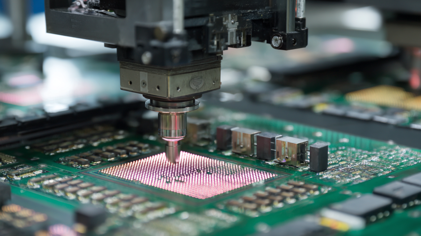
Industry Trends: Evolution of Wafer Probing Technology in Response to Miniaturization
As semiconductor technology continues to advance, the trend of miniaturization presents both challenges and opportunities for wafer probing techniques. According to a recent report by IC Insights, the semiconductor market is projected to grow from $527 billion in 2021 to $1 trillion by 2030, highlighting the urgent need for enhanced probing technologies. This evolution is driven by the demand for smaller, more efficient chips that can deliver higher performance while also reducing power consumption.
To keep pace with these industry trends, manufacturers are increasingly adopting advanced probing systems that utilize micro-sized probe tips and high-resolution alignment technologies. For instance, a report from Yole Développement indicates that the adoption of microelectromechanical systems (MEMS) in wafer probes could lead to a 20% increase in measurement accuracy, making it essential for tackling the complexities of next-generation semiconductor devices.
Tips: When selecting a wafer probing system, consider its compatibility with the latest chip designs and its ability to handle high-density layouts. Additionally, investing in systems with real-time data analysis features can greatly enhance testing efficiency and accuracy, ensuring that production yields meet market demands.
Related Posts
-

Tailored Solutions for Maximizing Reliability with Bed of Nails Test Fixtures in Electronic Testing
-

Tailored Solutions for Optimizing Your In Circuit Tester Performance
-

Understanding the Importance of Semiconductor Testing in Modern Technology
-
How to Maximize Efficiency in Wafer Probing Processes with Advanced Techniques
-
Understanding Micro Pogo Pins: The Key to Compact Electronic Connections
-
7 Best Features of Test PCB You Should Know
