Top 10 PCB Test Equipment Types for Global Buyers

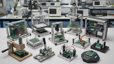
PCB complexity is rising across automotive, aerospace, medical, and data-center applications. Tighter tolerances make reliable inspection essential. PCB test equipment is no longer merely a final inspection accessory. It supports process control from bare-board verification to functional validation.

Prismark’s 2024 electronics industry report forecasts continued PCB market growth through 2029. However, regional demand and product mix create noticeable differences. IPC’s 2024 North American PCB Statistical Program also tracks changing orders, shipments, and business conditions. These findings show why global buyers should avoid purchasing decisions based on outdated capacity assumptions. The numbers are useful, but market forecasts are not perfect.

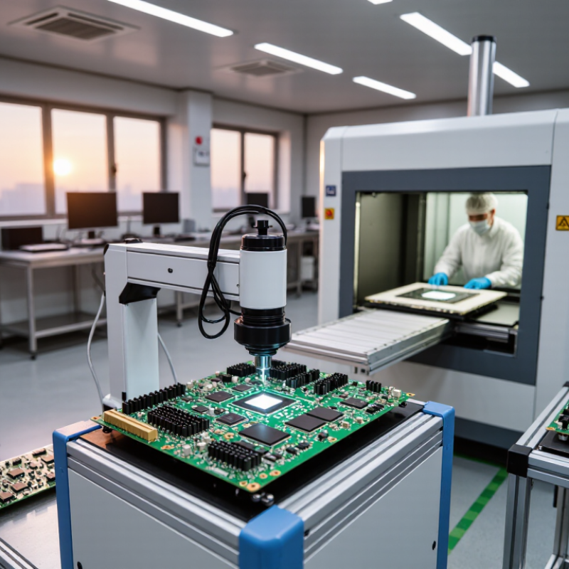
A modern factory may combine automated optical inspection, in-circuit testing, flying-probe systems, functional testers, X-ray inspection, and insulation-resistance equipment. Each method reveals different defects. A camera can identify solder bridges, while X-ray inspection can expose hidden voids beneath a BGA package. Flying-probe testing may suit prototypes, but high-volume lines often require faster fixtures. IPC standards, including IPC-A-600, IPC-6012, and IPC-TM-650, provide important references for acceptance and test methods. They do not define one universal machine for every factory.

This guide examines ten major PCB test equipment types for global buyers. It compares application, test coverage, speed, automation, maintenance, and ownership cost. Experience from production environments suggests that the cheapest instrument is rarely the least expensive choice. Calibration delays, software limitations, and poor technical support can quietly reduce output. Buyers should verify sample testing, data integration, operator training, and regional service coverage before approval. A practical decision leaves room for uncertainty. Every factory has different risks.
Top 10 PCB Test Equipment Types for Global Buyers

PCB Test Equipment Taxonomy: 10 Types, Test Goals, and Coverage Metrics

Top 10 PCB Test Equipment Types for Global Buyers

PCB test equipment should be classified by test goal, not only by machine name. Automated optical inspection checks solder joints, component placement, and polarity. Automated X-ray inspection reveals hidden voids, bridges, and barrel defects. Solder paste inspection measures paste height, area, and offset. In-circuit testers verify component values, opens, shorts, and test-point access. Flying-probe testers examine prototypes with limited tooling. Functional testers evaluate the assembled board under operating conditions. Boundary-scan systems test digital interconnects with limited physical access. Cable and harness testers measure continuity, insulation, and pin mapping. Burn-in systems expose early-life failures through controlled stress. Final quality stations combine electrical checks, visual review, and traceability records.

Coverage metrics make comparisons more reliable. Track defect coverage, false-call rate, escape rate, test yield, cycle time, and fixture utilization. The IPC 2024 Electronics Industry Survey continues to report supply-chain pressure and uneven production demand, making flexible test capacity valuable. Fortune Business Insights estimated the global PCB market at about USD 89.7 billion in 2023, with continued growth expected through the decade. That expansion increases the cost of undetected defects. Yet, coverage is never perfect. A high score can still hide poor programming or weak test access.

Tips: Match each tool to the board’s risk profile. Use SPI and AOI for process control, ICT for component-level faults, and functional testing for real-use behavior. Ask suppliers for measured escape data, not marketing claims. Review sample boards under production speed. Slower testing may improve accuracy, but it can quietly reduce factory output.

Electrical Test: ICT, MDA, Flying Probe, and Functional Test at 100% Net Coverage

Top 10 PCB Test Equipment Types for Global Buyers

Electrical Test: ICT, MDA, Flying Probe, and Functional Test at 100% Net Coverage

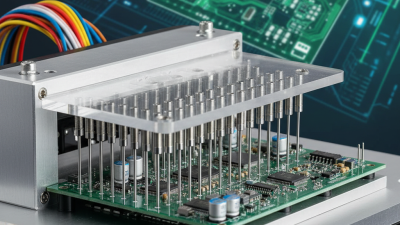
For global PCB buyers, electrical test equipment must match production volume, board complexity, and risk. In-circuit test (ICT) uses a dedicated fixture to contact test points and verify components, solder joints, opens, and shorts. Manufacturing defect analyzers (MDA) provide similar coverage with simpler test functions. Both work well for stable, repeated production. At 100% net coverage, every accessible net receives an electrical check. However, coverage does not guarantee that every defect will be found.

Flying probe testers use moving probes instead of a fixed fixture. They suit prototypes, engineering changes, and low-volume production. Setup is usually faster, but cycle times can increase on large boards. Functional testers power the assembled PCB and evaluate real operating behavior. They can reveal issues that passive electrical tests miss, such as communication failures or unstable power sequences. No setup is perfect. A board may pass basic checks and still fail under realistic loads.

Tips: Define test access during PCB layout, not after production begins. Request coverage reports with net-level details. Compare fixture cost, programming time, cycle time, and maintenance effort. In my experience, buyers often focus on purchase price and overlook false calls. I have seen rushed fixtures create unnecessary rework. Rechecking sample boards manually is slower, but it can expose weak assumptions before shipment.

Top 10 PCB Test Equipment Types for Global Buyers

Electrical Test: ICT, MDA, Flying Probe, and Functional Test in a 100% Net-Coverage Test Program

This capability map compares the primary test domains directly addressed by each equipment type. A value of 1 indicates direct coverage of the domain; 0 indicates that the domain is not the equipment's primary purpose. ICT, MDA, and flying-probe systems can be programmed for 100% net connectivity coverage when all accessible nets are included. Functional test validates powered product behavior rather than automatically guaranteeing 100% net coverage.

Imaging and Defect Analysis: AOI, AXI, Microscopy, and Microsection

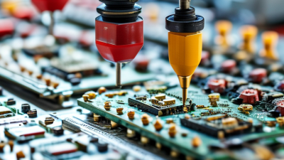
Printed circuit board buyers often compare test equipment by speed, resolution, and data quality. For imaging and defect analysis, the practical choices include AOI, AXI, microscopy, and microsection systems. Each tool reveals different failure evidence. AOI scans visible surfaces for missing components, solder bridges, pad damage, and printing shifts. It works well after assembly, but reflective solder can confuse the camera. False calls still require skilled review.

AXI examines hidden joints beneath packages and inside multilayer assemblies. X-ray images can expose voids, insufficient solder, broken vias, and misaligned internal structures. Choose equipment with suitable resolution, image enhancement, and repeatable inspection programs. A high-resolution image is not automatically useful. Operators must connect image patterns with process conditions and acceptance criteria.

Microscopy provides close visual evidence at component leads, solder fillets, and surface finishes. Measurements should include lighting control and calibrated scales, not only impressive magnification. Microsection analysis goes deeper by cutting, mounting, polishing, and examining a board cross-section. It can verify copper thickness, dielectric spacing, barrel cracks, and plating continuity. The method is destructive, so sampling plans matter. In my experience, one section can explain a recurring defect better than hundreds of automated alerts. Yet sample selection is imperfect, and a convenient cut may hide the real failure location. Good laboratories record settings, operator decisions, images, and limitations for every result.

Top 10 PCB Test Equipment Types for Global Buyers - Imaging and Defect Analysis: AOI, AXI, Microscopy, and Microsection

Rank Equipment Type Primary Inspection Method Typical PCB Defects Detected Typical Capability Production Speed Destructive Test Common Use Stage Relevant IPC References
1 2D Automated Optical Inspection (AOI) Visible-light imaging with pattern, geometry, and component comparison algorithms. Missing or misplaced components, polarity errors, solder bridges, opens, insufficient solder, lifted leads, and conductor-pattern defects. Non-contact surface inspection; capability depends on camera resolution, lighting, board design, and programming. High No After solder printing, placement, and reflow; also used for bare-board inspection. IPC-A-610, IPC-A-600, IPC-7095
2 3D Automated Optical Inspection (3D AOI) Structured-light, laser, or multi-angle imaging to measure surface height and volume. Solder-volume variation, insufficient or excessive solder, lifted leads, coplanarity issues, tombstoning, component height errors, and warpage-related defects. Provides height data in addition to 2D location and shape information; useful for fine-pitch and bottom-terminated components. High No Post-print process control and post-reflow assembly inspection. IPC-A-610, IPC-7095, IPC-7526
3 2D Automated X-ray Inspection (2D AXI) Transmission X-ray imaging that reveals internal solder joints and concealed structures. Voids, head-in-pillow defects, insufficient solder under packages, hidden opens, shorts, misalignment, and solder-joint anomalies beneath packages. Non-destructive internal inspection; image interpretation is affected by material thickness and overlapping structures. Medium to High No Post-reflow inspection of BGA, QFN, LGA, through-hole, and mixed-technology assemblies. IPC-A-610, IPC-7095, IPC-TM-650
4 3D X-ray Computed Tomography (CT) Multiple X-ray projections reconstructed into cross-sectional and three-dimensional volume data. Internal voids, cracks, hidden solder bridges, barrel defects, delamination, component damage, and complex interconnect failures. Detailed internal visualization with spatial resolution determined by system geometry, part size, and material density. Low to Medium No Failure analysis, process qualification, sampling inspection, and complex prototype evaluation. IPC-A-610, IPC-7095, IPC-TM-650
5 Stereo Optical Microscope Low- to medium-magnification three-dimensional visual examination with reflected light. Solder bridges, lifted leads, mechanical damage, contamination, scratches, poor wetting, and connector or component placement issues. Fast operator-assisted inspection of accessible surfaces; generally lower measurement repeatability than automated systems. Low No Incoming inspection, rework, repair, laboratory review, and operator training. IPC-A-610, IPC-A-600
6 Digital Video Microscope Camera-based magnified imaging displayed on a monitor, often with measurement and image-recording software. Fine-pitch soldering defects, conductor damage, scratches, residue, pad lifting, edge quality, and surface contamination. Good documentation and measurement convenience; accuracy depends on calibration, optics, lighting, and working distance. Low No Defect verification, rework inspection, process engineering, and quality documentation. IPC-A-610, IPC-A-600, IPC-DRM-40
7 Scanning Electron Microscope (SEM) Focused electron-beam imaging for high-magnification surface and fracture analysis. Microcracks, fractured intermetallic regions, dendritic growth, plating anomalies, contamination, and sub-micrometre surface features. Very high surface detail; samples may require preparation, vacuum compatibility, and conductive treatment. Very Low Usually No Advanced failure analysis, materials research, plating evaluation, and contamination studies. IPC-TM-650, IPC-6012, IPC-4556
8 PCB Microsectioning System Cutting, mounting, grinding, polishing, etching, and microscopic examination of a prepared cross-section. Plating-thickness variation, barrel cracks, hole-wall separation, resin recession, delamination, layer misregistration, and laminate defects. Direct cross-sectional evidence for multilayer construction and plated-through-hole quality. Very Low Yes Qualification, supplier audits, process validation, lot sampling, and failure analysis. IPC-TM-650 2.1.1, IPC-A-600, IPC-6012
9 Laser Surface Profilometer Non-contact optical or laser scanning to measure surface height, coplanarity, and topographic variation. Pad height variation, solder-joint profile issues, board warpage, surface irregularity, scratches, and connector coplanarity problems. Quantitative height and profile data; reflective, transparent, or highly textured surfaces may require controlled lighting and calibration. Medium No Board fabrication, assembly process control, connector inspection, and warpage characterization. IPC-TM-650, IPC-A-610, IPC-6012
10 UV and Infrared Imaging System Ultraviolet fluorescence or infrared-sensitive imaging for surface, thermal, and material-contrast analysis. Flux and conformal-coating residue, contamination, coating coverage variation, overheating zones, thermal hotspots, and some material anomalies. Useful for contrast enhancement and thermal investigation; results depend on emissivity, coating chemistry, temperature, and illumination. Low to Medium No Cleaning verification, conformal-coating inspection, thermal troubleshooting, and failure analysis. IPC-CC-830, IPC-TM-650, IPC-A-610

Note: Capability, speed, and resolution are typical application-level descriptions rather than guaranteed equipment specifications. Actual performance depends on board size, component density, materials, inspection programming, calibration, and acceptance criteria.

Signal Integrity and Safety: TDR, VNA, HiPot, and 50 Ω Verification

Reliable PCB testing starts with matching the instrument to the failure you need to see. A time-domain reflectometer, or TDR, sends a fast edge through the trace. It reveals impedance changes as distance, not just as a pass-or-fail result. On a 100 mm differential pair, an unexpected bump may indicate a connector transition, an uneven reference plane, or excess via stubs. I always verify cable delay before judging the board. Small setup errors can look like real defects.

A vector network analyzer, or VNA, measures insertion loss and return loss across frequency. It helps confirm whether a high-speed channel maintains controlled impedance under operating conditions. Calibration at the cable ends matters. So does fixture quality. I have seen a clean-looking PCB produce poor data because the test fixture was poorly launched. The instrument was not the real problem. That mistake remains easy to repeat.

HiPot testing addresses electrical safety rather than signal quality. It applies a controlled high voltage between selected conductors and checks insulation integrity. Test voltage, ramp time, leakage limits, and discharge procedures must follow the applicable product requirements. Never treat HiPot as a substitute for functional testing. For 50 Ω verification, use a calibrated termination, short path, and suitable probe. Check resistance with a meter, then confirm high-frequency behavior with a TDR or VNA. A nominal 50 Ω reading at low frequency can still hide serious discontinuities. Measurements need context.

Global Buyer Criteria: IPC-A-600 Classes 2–3, IEC 61189, GR&R, and ROI

Top 10 PCB Test Equipment Types for Global Buyers

Global PCB buyers should match test equipment with IPC-A-600 Class 2 or Class 3 acceptance levels. These classes affect inspection depth, defect tolerance, and reporting detail. A flying-probe tester suits low-volume boards and frequent design changes. In-circuit testers support stable production with repeatable fixtures. Automated optical inspection checks solder joints, spacing, and component placement quickly. X-ray inspection reveals hidden voids, opens, and insufficient solder under packages.

Other useful equipment includes bare-board testers, boundary-scan systems, functional testers, insulation resistance testers, hipot testers, and thermal cycling chambers. IEC 61189 methods help define electrical, mechanical, and environmental test conditions. Buyers should request traceable calibration records, controlled software versions, and test-result storage. A clear report should show the board identity, operator, date, limits, and failure location.

GR&R deserves attention before equipment approval. A measurement system may repeat results but still measure the wrong feature. That mistake is expensive. Test a representative sample across operators, shifts, and board conditions. A result below the customer’s internal variation target is useful, but acceptance criteria must be agreed before purchase. ROI should include fixture costs, labor, retest rates, maintenance, training, and avoided field failures. Cheap equipment can become costly when false calls slow production. Real factory data is better than a polished quotation, though early estimates are often imperfect. Recheck them after three production months.

Go to Top